Some
Details about the
PC (Personal Computer)
Boot-up Sequence
Copyright © 2006, 2007
by Daniel B. Sedory
NOT
to be reproduced in any form without Permission of the Author!
NOTE:
This page is still under construction; if a topic doesn't make sense,
you may contact us for more information.
What
happens When a PC Powers-up?
When you turn it on, a computer's
power supply must bring all the separate voltages required by the Motherboard
and peripheral components to an acceptable level with enough current to power
the whole system. These voltages include both + and - (plus and
minus) 12.0 V (volts), + and - 5.00 V and most likely
+3.30 V (which may be reduced even further by circuits on the motherboard
for the latest power efficient processors). [ Note: All
these voltages will vary slightly for each combination of power supply, motherboard,
disk drives and various peripherals (since all electronic components drawing
current will alter the power supply's load), but they should never
fluctuate by much (if at all) upon reaching their operating levels. If
a power supply isn't quiet enough (i.e, it has too much AC noise
on any of its outputs), the motherboard's BIOS chip may not function
correctly; or more likely, the Memory portion of the Power-On Self Test will
fail. Either way, the system will never boot up completely! In locations where
the AC input from the power company experiences occasional problems or total
loss thereof, devices which store up power for a some minutes, allowing you
to save your data and properly shut-down the system, should be used. ]
Due to the sensitive
nature of some IC chips (Integrated
Circuits inside small metal, ceramic or plastic packages),
especially the CPU (Central Processing Unit; which
produces a great deal of heat, thus the reason for a large metal heatsink
and fan on it), the motherboard may never be allowed to power up until a power
good signal is received from the power supply. This may take over half a
second; a tremendously long time when compared to the speed of a CPU that can
step through millions of instructions per second (MIPS), yet it often
seems almost instantaneous to its human operator.
By the time you notice the
sound of a fan rotating or drive motor spinning up, the voltages have
already stabilized, power has been applied to all the chips (the
interface chips that facilitate communications between the CPU and the
Memory modules; along with any audio, video or LAN cards plugged into
bus connectors, and the controllers for peripheral devices such as keyboard,
mouse, hard disk and CD/DVD drives)
and the motherboard's Clock-pulses are already synchronizing all those
interactions. In
what feels like a fleeting moment to us, the PC is already executing
instructions from the BIOS
(Basic Input/Output
System) chip,
and a short time
later
a speaker or transducer built into the computer's chasis
beeps once signaling the POST (Power-On Selt
Test) has completed without any errors.
The BIOS in Detail
Virtually every
PC, since the very first IBM® Personal Computer produced in 1981
to the latest Intel® or even AMD® based PC, has had exactly the same
Memory address hard-wired into its CPU as a reference for
its first instruction! This means every PC's CPU will always begin executing
machine code instructions from essentially the same location inside any
BIOS chip used to boot-up the system. That address is:
F000:FFF0 (in Segment:Offset notation) or:
FFFF0h (in
Linear notation). You may also find it represented by
FFFF:0000 [as
it was recorded in IBM's
original Technical Reference manual; P/N 6025008]
or as just FFFF:0
(in Normalized Segment:Offset notation). [To understand
why the Segment:Offset pair F000:FFF0 is also equivalent to FFFF:0,
read this page on
Memory Segments.]
IBM®
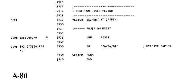
named this address the "Power On Reset Vector " and it
always contains a far jump instruction to
the beginning of the BIOS chip's Power-on RESET code. Here's a display of what
you'd find in that location and the next 12 bytes of an original IBM®
PC's BIOS code:
Offset: 0  1  2  3  4  5  6  7  8  9  A  B  C   ASCII chars.
------ ---------------------------------------  -------------
0FFFF0 EA 5B E0 00 F0 30 34 2F 32 34 2F 38 31  .[...04/24/81
|
The first five bytes (shown
in green) comprise the Power-On Reset Far Jump code which is essentially
'set in stone' for all PC BIOS chips. The Assembly source code
for these 5 bytes is:
JMP F000:E05B (as you can see, Segment F000:
is embedded inside this instruction, so that's why its location is often
listed as F000:FFF0). The next eight bytes (shown in yellow) were
originally called the "RELEASE
MARKER" by IBM®;
they always contain the release date of the code (which was
04/24/81 for those
first PCs).

Portion of page A-80, Appendix A, "ROM BIOS Listing," in the Technical
Reference manual
(IBM Part Number, 6025008), First
Edition (August, 1981), of the IBM Personal Computer
Hardware Reference Library. (Note:
Click on pic; larger size is available.)
Note: In the original "IBM
Personal Computer Technical Reference Manual," there was an error in the
code listing for the address of the RESET CPU test code. It should have been
listed as: "0000 EA5BE000F0"
instead of what you see in the picture above. If you check the address shown
on page A-5, it's obvious "RESET"
begins at the Segment:Offet address of "F000:E05B".
If you're running any Microsoft/IBM
OS from DOS through Windows Vista, you should be able to perform the following
DEBUG commands (Windows users must first click on start ->
Programs -> Accessories -> Command prompt to open a DOS window), and
obtain results similar to the following (DEBUG.EXE should be in your path):
C:\>debug
-d f000:fff0 [To 'dump'the last 16 bytes of memory Segment.]
F000:FFF0  EA 5B E0 00 F0 30 34 2F-31 34 2F 30 33 00 FC 48   .[...04/14/03..H
-
-u f000:fff0 l5 [The "l5" stands for 'length of 5 bytes.]
F000:FFF0 EA5BE000F0    JMP     F000:E05B
-
-q [To exit DEBUG. This is a Q for 'Quit'.]
|
ENTER the commands shown
in green
at the DEBUG prompt (a "-"). On this particular computer, we have
the same Jump instruction as the original PC, but this BIOS code was
released on April 14, 2003 ("04/14/03"). (For more on the use
of DEBUG, see our Guide to MS-DEBUG).
[ NOTE: The author is presently
unsure about the following sentence! This must be answered: "Was the original
PC limited to executing BIOS code only from the actual chip itself, or were
the instructions first copied into RAM for later execution?" ] Since
the original PC had far less than a binary Megabyte of memory
(zero through FFFFF
in hex = 1,048,576 bytes), executing
its BIOS ROM (Read-Only Memory)
instructions meant the motherboard had to access the requested code through
the pins of its BIOS chip every time. But as PC memory grew to 1 MiB
and beyond, the ROM code was then cached (or shadowed)
in faster and larger memory modules (often 512 MiB or more for present systems)
where the code could possibly be patched (changed)[1]
with some alternate code.
How to View the BIOS code
Footnotes
1[Return
to Text] Note, however, that almost any BIOS code you'll encounter has been
able to write-protect itself in memory for many years! It does this by incorporating
checks of any low-level BIOS routines that could be used to alter memory locations,
and simply disallows writes to where the BIOS is shadowed in memory. If any
portion of the BIOS code must be changed, for example by an operating system,
a programmer must use hardware code which directly accesses the memory chips
or somehow avoids the write-protection routines of the BIOS.
Last Update: 15 December 2007 (15.12.2007).
You can write to me using this: online
reply form. (It opens
in a new window.)
 MBR and Boot Records Index
 The Starman's
Realm Index Page
