Papers in the field of chemistry and physics usually become obsolete soon, especially those concerning semiconductors.

The following one, however, has some special features. To begin with, it explains the behaviour of the glorious old crystal detector, the first device to make radio signals audible.
This study was the by-product of a wider investigation on the strange behaviour of the empirical correction factor for spreading resistance measurements, which learned us a lot about the factors influencing the reliability of that method. In addition this paper applies to all methods using pressure contacts on semiconductors.

With the steadily decreasing dimensions in modern semiconductor devices, however, it becomes also important, that it explains how the semiconductor band gap and consequently the barrier height of PN-junctions will be influenced when touched by stress fields from the surface.

Back to: english.htm


Appl. Phys. Lett., Vol. 20, No. 11, 1 June 1972 420
Position of the Band Edges of Silicon under Uniaxial Stress
 
P. Kramer and L. J. van Ruyven
Semiconductor Development Laboratory, N. V. Philips Gloeilampenfabrieken, Nijmegen, Netherlands
(Received 22 December 1971; in final form 17 March 1972)
  Schottky barrier heights of metal-silicon contacts have been measured as a function of temperature at high uniaxial <lll> stress (100 kbar). The change in band gap, as compared to the zero-pressure band gap, can be attributed to a change in position of the conduction band edge alone, i. e. , a change in electron affinity.  
The temperature dependence of the zero-bias resistance of point contacts on a number of silicon samples has been measured. The point contacts were obtained by pressing two tungsten ruthenium alloy probes, having a tip radius of curvature r = 25 µ, perpendicularly on a <111> polished surface of the samples with a load of 35 g. Application of the Hertzian formulas1 and the silicon elastic limit of about 1000 kg/mm2, as assumed from microhardness measurements,2 gives a radius a = 2.6 µ for the resulting plastically deformed imprint, corres-


  421
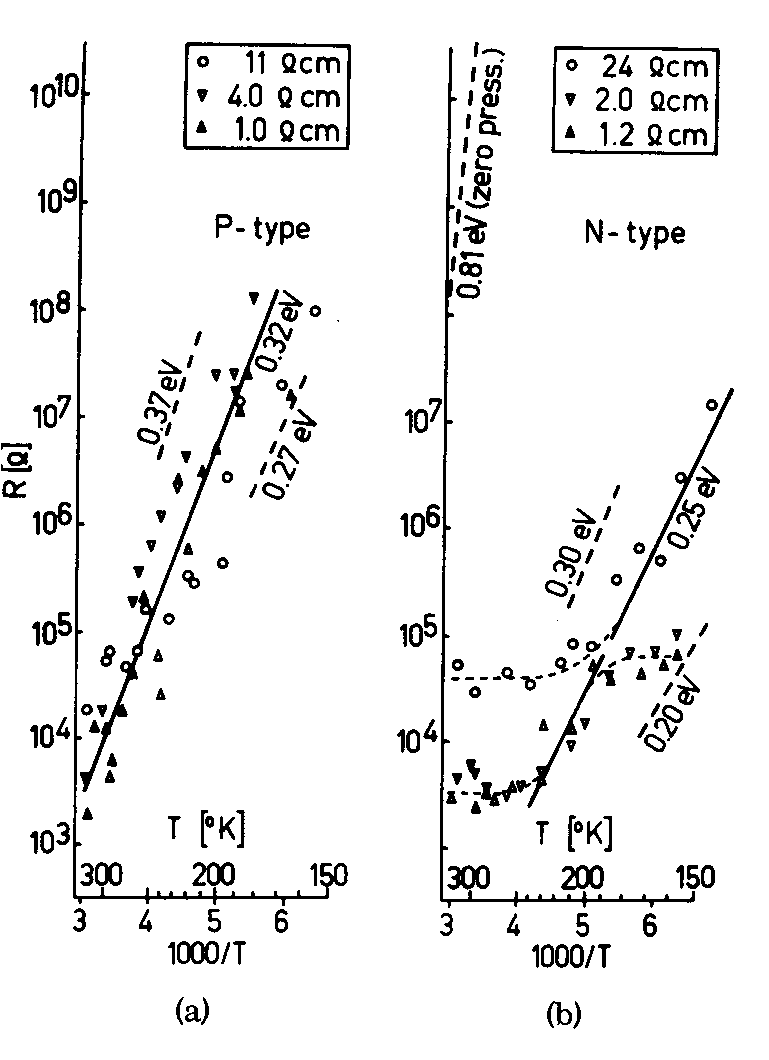
FIG. 1. (a) Contact resistance R versus temperature T for a RuW probe on p-type silicon for different resistivities. The straight lines indicate the behavior of potential barriers of different heights.
(b) The same for n-type silicon.

ponding to a contact area of 21 µ2. Because a << r, the pressure at the contact interface can be considered to be uniaxial.

This contact has been investigated and is assumed to be a pure metal-semiconductor contact due to the high pressure. The resistance between the two probes is measured at different temperatures T between 150 and 325°K and the resistance per probe is plotted on a logarithmic scale as a function of 1000/T in Figs. l(a) and l(b) for p- and n-type silicon, respectively. The p-type samples show a logarithmic behavior over almost the entire temperature range, as indicated by the solid straight line. For the n-type samples, this occurs below 250 °K.

This logarithmic behavior can be attributed to thermal emission over a potential barrier. The zero-bias resistance Rb due to thermal emission can be calculated by taking the derivative of the Richardson equation3 at the point V= 0, which gives

 
Rb =
___k___
qA**TA
exp
Eb
kT
(1)

in which k is Boltzmann's constant, q is the electron charge, A** is the effective Richardson constant (32 Acm-2 °K-2 for holes, and 112 Acm-2 °K-2 for electrons, T is the absolute temperature, A is the contact area, and Eb is the barrier height the electron has to surmount in passing from the metal into the silicon.

The solid line in Fig. l(a), corresponding to an activation energy of 0.32 eV, represents the behavior of the barrier for p-type samples. Although this line appears to be perfectly straight in the figure, in reality a slight curvature is present, due to the temperature dependence of the preexponential factor in Eq. (1). However,

the scale of the figures is such that this cannot be noticed. According to Eq. (1), the barrier height Ebp =Eb equals 0.32 eV for the three samples presented, having a resistivity of 11, 4.0, and 1.0 Scm, respec- tively. The n-type samples (of 24, 2.0, and 1.2 Scm, respectively) show a logarithmic behavior (correspon- ding to a barrier height Ebn = Eb of 0.25 eV) only below 250 °K. Above 250 °K the contact resistance is determined by the resistivity of silicon, as shown in Fig. l(b). The accuracy of the separate measurement points is indicated in Figs. l(a) and l(b) by dashed straight lines, yielding an uncertainty of ± 0.05 eV for the height of the barrier. For the sake of clarity the actual data are given for those samples (>= 1 Scm), in which no corrections on the barrier height have to be applied. Measurements on silicon samples having a resistivity of 0.35, 0.092, and 0.030 Scm (p type) and 0.098 and 0.028 Scm (n type), respectively, also yield a barrier height of 0.32 or 0.25 eV, respectively, if corrections for barrier lowering according to Ref. 3 are applied.

The total band gap is equal to the sum of both barrier heights, being the energy difference between the respective band edges and the Fermi level at the interface.4 Thus, under the stress we applied, the total band gap Eg amounts to 0.32 + 0.25= 0.57 eV (±0.1 eV), resulting in a change )Eg of 1.11 - 0.57 = 0.54 eV ( ± 0.1 eV) with respect to the zero-pressure band gap of 1.11 eV at 300 °K. This )Eg is large compared to the temperature dependence of the band gap (0.04 eV over the total temperature range we applied,5 which is therefore neglected.

At the metal-silicon interface, the uniaxial pressure Po is equal to the silicon elastic limit of about 1000 kg/ mm2 (100 kbar). However, this is only true at depths z that are small with respect to the contact radius a because of the hemispherical pressure distribution. The pressure Pz in the z direction decreases according to the relation6

 
Pz =
__a2__
a2 + z2
Po
(2)

It has been assumed that the effects due to the band-gap

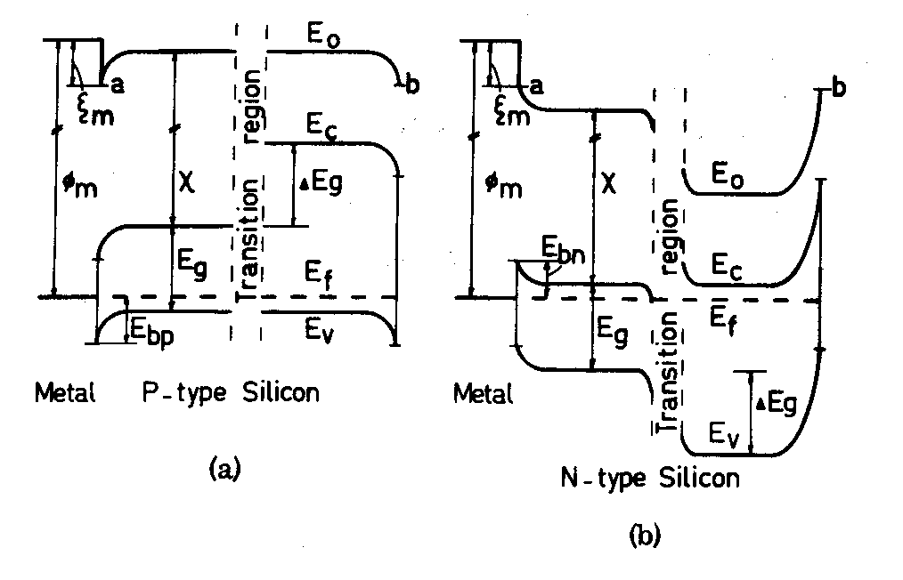
FIG. 2. (a) Energy-band profile of the metal probe on p-type silicon. The transition region separates the compressed (left- hand side) and uncompressed (right-hand side) part of the silicon.
(b) The same for n-type silicon.


422
variation as a function of position can be separated from the barrier because the depth z of the space-charge layer that determines the zero-bias resistance is small with respect to the contact radius a.

It appears that the band-gap change measured in this way agrees well with the results of others; Balslev7 measured a change )Eg of 0.035 eV at 100 kg/mm2, while Bulthuis8 found a pressure dependence of -5 x 10⁻⁴ eV kg-1 mm2 in the range f rom 200 to 800 kg/mm2.

The important experimental observation is that in all P-type samples, independent of resistivity, the barrier is unaffected by uniaxial <111> stress, and its value as determined from the thermal activation energy [see Fig. l(a)] is identical to the zero-pressure value, 1.11 - 0.81 = 0.30 eV, 9 within the limits of observation. From this we conclude that the energy difference between the Fermi level and the valence band edge at the interface remains unchanged under uniaxial <111> stress.

This observation is fully supported by our pressure ex- periments on the n-type samples of various resistivities. The barrier of the n-type samples shows a substantial decrease under uniaxial <111> stress, equal to the total change in band gap. This can be seen in Fig. l(b), where the measurements on three different samples yield a barrier height of 0.32 eV, while the zero-pressure value on vacuum cleaved surfaces amounts to 0.81 eV.9 The zero-bias resistance of the n-type zero-pressure barrier is also indicated in Fig. l(b) for comparison by a dashed straight line (note the high level of resistance).

The system can be considered as a metal-semiconductor contact on top of compressed silicon which gradually changes to silicon under zero pressure with well-known properties. Figure 2 shows both cases. For p type, Fig. 2(a) gives on the left-hand side a representation of the energy-band diagram of the metal to compressed silicon contact, which via a schematically drawn transition region is connected to the bulk silicon. The work function of the probe metal is denoted by Nm, and the electron affinity of the silicon by P. >m represents a dipole equal to the difference in work function of the metal and the semiconductor surface, while Eo gives the position of the vacuum level, defined as the energy of an electron with zero kinetic energy, which is just outside the crystal. The position of Eo is indicated because its slope is a measure for the built-in electrostatic field, independent of band-bending effects due to changes in the band gap. At thermal equilibrium there is no potential difference across the semiconductor, and hence the level a of the vacuum at the interface should be equal to its level b at the noncompressed surface. Therefore, taking into account that the barrier height and, consequently, that the band bending on the left- and right-hand sides are equal lor P-type silicon, it follows that the positions of Ev and Eo do not change in the transition region, while Ec changes over an amount )Eg.

The energy-band diagram for the contact on n-type sili- con is shown in Fig. 2(b). In this case, the band bending at the noncompressed surface is much higher than that at the compressed interface, and consequently Eo and Ev are changed while Ec remains constant. Note that, on p-type as well as on n-type silicon, P is increased by an amount )Eg, due to pressure.

The Fermi level at the interface is assumed to be determined by the charge of a high density of surface states within the band gap.4 From the distortion of the periodical potential, Pugh10 calculated the distribution of surface states for diamond, which showed a strong maxi- mum slightly below the center of the gap. For a charge- neutral surface these states would be half full, which would result in an interface Fermi level at about one-third of the band gap. This has been verified experimentally for a large number of semiconductors with band gaps ranging f rom 0.25 to 10 eV.4

It is a remarkable fact that the "one-third rule", which is so generally obeyed at zero pressure, is apparently invalid in silicon under <111> uniaxial stress. The in-variance of the energy difference between the Fermi level and the valence band edge has been earlier observed by Crowell et al.5 for band-gap changes due to temperature. They measured the Schottky barrier height on n-type silicon at zero pressure and found a decrease with temperature exactly equal to the total silicon band-gap decrease. This observation has been confirmed by Aspnes and Handler.11 The band-gap decrease due to temperature changes or pressure changes is apparently in both cases a change in position of the conduction band gap [=edge] alone, the latter being an order of magnitude larger.

A very recent article12 on n-type GaAs under hydro- static pressure reports a barrier height increase equal to the band-gap increase rate and also concludes that the Fermi level at the interface remains pinned with respect to the valence band edge when the pressure goes up.


1S. Timoshenko and J. N. Goodier, Theory of Elasticity (McGraw-Hill, New York, 1951), p. 372 ff.
2A. A. Giardini, Am. Mineralogist 43, 957 (1958).
3J. M. Andrews and M. P. Lepselter, Solid-State Electron. 13, 1011 (1970).
4C.A. Mead, Solid-State Electron. 9, 1023 (1966), and references given therein.
5C. R. Crowell, S. M. Sze, and W. G. Spitzer, Appl. Phys. Letters 4, 91 (1964).
6K. Bulthuis, Philips Res. Repts. 20, 415 (1965).
7I. Balslev, Phys. Rev. 143, 636 (1966).
8K. Bulthuis, Philips Res. Repts. 23, 25 (1968).
9M.J. Turner and E. H. Rhoderick, Solid-State Electron. 11, 291 (1968).
10D. Pugh, Phys. Rev. Letters 12, 390 (1964).
11D. E. Aspnes and P. Handler, Surface Sci. 4, 353 (1966).
12P. Guétin and G. Schréder, Solid State Commun. 9, 591 (1971).


1