A FULLY MAINS OPERATED SOLID STATE POWER DELAY CIRCUIT
V.Vidyalal, V. Sivanand and K. Rajasree,
Floyds Inc., "KAILAS"
EDAKKAD P.O, CALICUT,
INDIA - 673005
Or
V.Vidyalal
Uni-Tel. Inc, 8111 LBJ Freeway, Suite 1100
Dallas, Texas-75251,
USA
lal@uni-tel.com
Introduction
This circuit can be used to turn off appliances, porch lights, or any other load after a certain time interval. The unique features of this circuit are 1) Light Weight 2) Fully mains operated 3) Uses fully solid state components (Hence no maintenance required in the long run) 4) Inexpensive 5) Low stand by current and 6) Silent operation because of solid state switching.
For driving heavier loads all one need is to substitute an appropriate triac leaving the rest of the circuit unaltered.

THE CIRCUIT
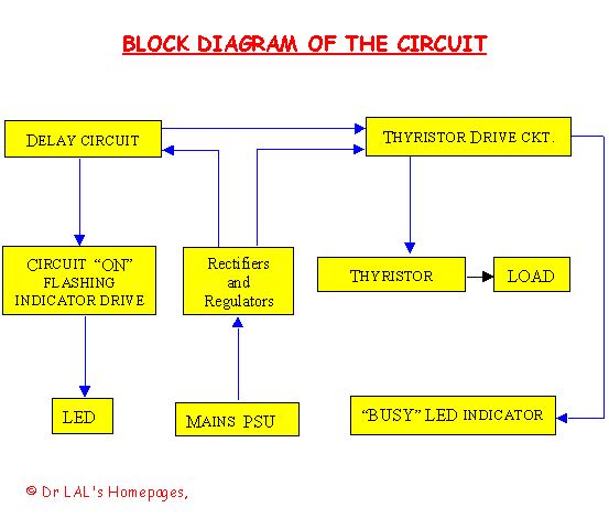
The circuit can be basically divided into four major parts :-
OPERATION: Testing is very simple. First switch on the power supply using S1. LED2 starts flashing, the rate depending on R11. Adjust R11 (with a plastic trimming tool) according to the user’s requirement. Press S2. LED1 should light up and when S2 is released, LED1 should remain lit for some time depending on the value of R6 (adjust R6 for the required time). When LED1 lights up, the triac is sure to fire and energize the load. After a short interval of time the load is disabled.
PARTS LIST
Semiconductors:
IC1 - 7809, 3 Pin voltage regulator. IC2 - CD4049B CMOS TRIAC - According to load current requirement
Q1 - BC 548B NPN Transistor D1, D2 - IN4007 Silicon Diodes
RESISTORS:
(ALL ¼ W, 5% Carbon, unless otherwise specified.)
R1 = 100 , 5W R2 = 100 , 1W R3 = 1k2
R4 = 330 R5 = 1M R6 = 1M Preset
R7 = 10M R8 = 100 R9 = 1M
R10 = 2M2 R11 = 1M Preset R12 = 680
CAPACITORS:
C1 = 2.2m F/400 V, Metallised Polyester C2 = 100nF/400 V, Polyester
C3 = 1000m F/50V Electrolytic C4 = 100nF/50V, Ceramic
C5 = 1000m F/50V Electrolytic. C6, C7 = 100nF/50V, Ceramic.
C8 = 47m F/12V, Tantalum bead. C9 = 1m F/50v, Polyester.
SWITCHES:
S1= SPST SWITCH, S2 =PUSH BUTTON SWITCH
MISCELLANEOUS:-
Fuse = 1A, slow blow, LED1 = Green, LED2 = Red, flexible wires, mains cord, mains socket, LED holders etc.
CAUTION
: Since the whole circuit is connected to the live mains, one should be extremely careful. It is advisable to enclose the whole unit inside a plastic cabinet, leaving provisions for input and output cables.*-*-*-*-*-*-*-*-*
NOTES
WARNING AND DISCLAIMER
(!!!!!!!)Mains-powered and also equipment like the one described above contains high AC voltages. These can be potentially lethal. If you do not know how to safely handle the inside of equipment containing high voltages, please do not attempt to open the equipment. Before carrying out any work inside equipment containing high Voltages, ensure that you disconnect the Unit from the Mains. (2) The information included herein is provided as-is, with no warranties expressed or implied. No responsibility on the part of the author is assumed for the technical accuracy of the information given herein or the use or mis-use of said information.
The equipment described in this article was designed, fabricated, and tested spending my own personal time and using my own personal resources.
The information on this site is Copyright © 1998 of Dr.LAL. You may link to these pages or print them out for your own personal use, but no parts of these pages can be reproduced, sold, or transmitted in any form without my explicit written permission. By copying or paraphrasing the intellectual property on this page, you're automatically signing a binding contract and agreeing to be billed $1000 payable immediately. © Dr LAL's Homepage (CKT.DESIGN) 1998.
HOME ` FOR THE INDEX AGAIN !.....