NOTE: This page is still in a somewhat rough condition. The writing, I believe, may not be clear enough in some places, and some of the graphics need to be added or tidied up. The basic ideas should all be here, however, and what's missing should be fairly easy to grasp through intuition. If you have any ideas on how this page ought to be modified (or if you want to draw nicer-looking diagrams for anything), let me know. Thanks!
Although basic computer RAM is a relatively simple device compared to the digital devices that get most of the attention nowadays, the internal structure of RAM is not well understood, and since RAM is such a crucial component of any device that uses a digital microprocessor, it's in the microcomputer/microelectronic technician's best interests to understand RAM.
This page will focus mainly on SRAM (Static RAM). SRAM retains the values you put in it, unlike DRAM (Dynamic RAM), which needs to be refreshed several times every second. The only real advantage DRAM has over SRAM is that it's much cheaper, so it's necessarily used for the main system RAM on most PCs. (If RAM manufacturers used SRAM for main PC RAM, the RAM in your computer would probably cost more than the CPU!) DRAM sucks, however, because the fact that it needs to be constantly refreshed makes it hugely annoying to work with. So, SRAM it will be!
On the outside, SRAM chips are pretty simple. Aside from address bus and data bus pins and two power pins, there are only three other pins on a typical SRAM chip: Chip Enable (CE), Output Enable (OE), and Write Enable (WE). On the inside, all RAM chips consist mainly of a big grid of RAM cells, tiny devices which are each capable of storing a single bit. (Of course, the RAM cells are organized into bytes. Typically, 8 bits make a byte, although this is not necessarily the case.) So we see that all an SRAM chip really has to do is use the address sent to it to select a single byte-sized line of RAM cells, enable all those cells, and if it's writing to memory, to change what's stored in those cells. A short enough explanation, but each step of the process involves devices which contain many smaller devices.
Let's start with the most fundamental part of an SRAM chip: A RAM cell. In SRAM, the RAM cells are basically D-type flip-flops, so to understand RAM cells, you need to understand D flip-flops. Before we get into D flip-flops, however, you need to understand...
The set/reset latch is the most basic latch circuit. A latch is a digital electronic logic circuit which, upon receiving an instruction to change its output, will "latch" the output, so that the output does not change even after the input has been removed. The set/reset (S/R) latch looks like this internally:
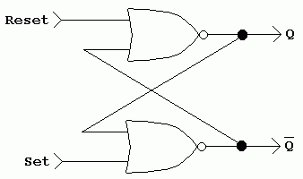
The S/R latch has two inputs and two outputs. The two inputs are labeled "Set" and "Reset". Set, when enabled, turns on the latch, and Reset turns it off. The two outputs are labeled Q and /Q. (The Q with the line over it in the diagram means "NOT Q", or the inverse of Q. Since there is no way to create a line over a character in text, usually the convention of preceding a signal with a slash is used to indicate "NOT".) Q is the main output for the latch. When the latch is on, Q will be 1. When the latch is off, Q will be 0. /Q is the opposite of Q, so when Q is 1, /Q will be 0, and vice-versa.
Not that this is an active-high S/R latch, meaning that its inputs trigger when they go high. It's possible to make an active-low S/R latch by replacing the NOR gates with NAND gates, but we won't get into that now.
As you can see, when Set goes high, the output of the NOR gate on the bottom must be 0 (because when either NOR input is high, the output is 0). This sets /Q to 0. This same 0 goes to the lower input on the NOR gate at the top; Since Reset must be low (since Set is high), both inputs to the NOR gate at the top are 0. Therefore, since both inputs are 0, it outputs a 1. This 1 hits the top input of the bottom gate, keeping the gate on (and setting Q to 1), and the latch remains stable in this state until Reset goes high. Similarly, the opposite happens when Reset goes high. The workings of this latch may seem confusing at first, but if you follow the logic paths you should be able to understand it clearly.
The R/S latch is the basis for most digital flip-flop circuits. Once you understand it, you can move on to...
The D flip-flop is quite a simple digital device with four pins; Two of these pins are inputs, and two are outputs. The chief input is the D (Data) pin, which, like any other digital signal, can receive either a 1 or a 0. The other input is the E (Enable) pin, sometimes labeled the Clock or Clk pin. The two outputs are Q and /Q (NOT Q, or the inverse of Q). However, within RAM, the /Q output of a D flip-flop is not used, and thus the flip-flop can, for purposes of using it in RAM, be reduced to a three-pin device with two input pins and one output pin. A simple enough device, indeed.
The operation of the D flip-flop is simple: The Q output reflects the D input. When the Enable or Clock pin is activated, the state of D is stored in Q. Once this happens, Q stays the same and does not change, regardless of the state of D, unless the Clock pin is triggered again. The D flip-flop thus acts as a single-bit memory storage unit: When you want to store a bit in it, you set D accordingly and pulse its clock. Once this is done, its Q output will reflect the bit stored in the flip-flop until you change it.
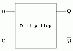
Internally, the D flip-flop is basically an R/S latch with some additional circuitry added to the inputs.
Note that D flip-flops are usually "edge-triggered", meaning that they will change their state only in the moment that the Clock pin is enabled. The D flip-flop diagrammed here is not edge-triggered; The output will follow the input as long as the Clock pin is enabled. There's nothing really wrong with this in terms of using the flip-flop for RAM. We could turn it into an edge-triggered device with some more gates, but that's not necessary now.
The D flip-flop is a great device, but to make it more useful, it should come equipped with an Enable pin. Many D flip-flop chips do have Enable pins, but in keeping with the theme of illustrating the internals of these devices, it's appropriate to show you...
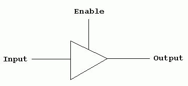
In digital logic design, you can add an Enable signal to just about any digital signal by simply running it through a tri-state logic buffer. A digital logic buffer is just a device that takes whatever digital logic is fed into it, and outputs the exact same signal. (Sort of like a NOT gate, except without the inverting part.) A "tri-state" digital device is one which includes an Enable pin, so that you can enable or disable the output. When the Enable pin is turned off, the output goes into a "high-impedance" state in which it is essentially a dead pin, disconnected from the rest of the device. The digital logic symbol for a tri-state logic buffer looks like this:
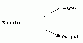
At the component level, a tri-state digital logic buffer is really just a single transistor. The base of the transistor acts as the Enable pin, the transistor's Collector is the logic input, and the Emitter is the logic output. Thinking about it in this way, the tri-state logic buffer would look like this:
Now that we know how to make a D flip-flop and put an Enable pin on it, we have...
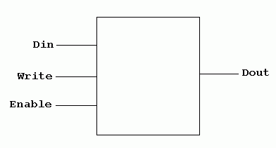
A typical RAM cell has only four connections: Data in (the D pin on the D flip-flop), data out (the Q pin on the D flip-flop), Write Enable (often abbreviated WE; The C pin on the D flip-flop), and Output Enable (the Enable pin which we added). Now that we have this concept, we can black-box it, which, for simplicity's sake, I will do on this web page from this point henceforth. Our RAM cell, made into a logic block, looks like this:
If you've understood everything thus far, you're almost done with understanding how SRAM works. You already know how one individual memory cell works, so now the trick is to just arrange them in an array so that you can address each one independently. To do this, we need to be able to take memory addresses and use them appropriately, so the next thing we'll learn is...
An address decoder is a device which reads in a binary-represented memory address, and based on the address it receives, turns on a single output. If an address decoder has n inputs, then it will have 2^n (2 to the power of n) outputs. At any point in time, only one output line is on, and all the others are off. The decoder must have a separate output for every byte in memory. Since a byte is 8 bits (usually), and every RAM cell is one bit, each output from the memory decoder goes to 8 RAM cells.
For simplicity's sake, we'll illustrate two small-scale memory decoders: The 2-to-4 decoder, and the 3-to-8 decoder. In reality, a modern RAM chip would have much larger decoders than this; An 8 kilobyte RAM chip (which is quite small by today's standards) would have a built-in 13-to-8192 decoder, but trying to draw that and represent it here on this website would probably be overkill.
An address decoder is a form of combinatorial circuit; The idea behind it is that for every possible combination of inputs, there needs to be a separate output that will activate. For example, suppose we have a 2-to-4 decoder; This is a decoder with two inputs and four outputs. The idea is that for every possible combination of 1s and 0s on the two inputs, a different output needs to activate. There are four possible ways to put 1s and 0s on two inputs: 00, 01, 10, and 11. If we call the inputs "in0" and "in1" and the outputs "out0" to "out3", then the 2-to-4's truth table looks something like this:
in0 in1 � out0 out1 out2 out3
�����������������������������
0 0 � 1 0 0 0
�
0 1 � 0 1 0 0
�
1 0 � 0 0 1 0
�
1 1 � 0 0 0 1
The circuit diagram for a decoder might look complicated at first, but actually, it can be pieced together from a pretty simple idea, so just before I show you the diagram for one, let me try to explain the concept: To make a decoder, you attach two wires to each input. One wire simply comes directly from the input, while the other wire passes through a NOT gate (an inverter, which sets a logic 0 to a 1, and vice-versa). Once this is done, you have something that looks like this:
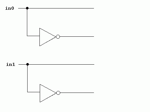
After this, take one wire from each input, and connect the ends of them to an AND gate. The output of the AND gate then becomes one of the address decoder's outputs. Add different AND gates for each possible combination of inputs, and you're done. Each outputting AND gate must have a different combination of input triggers. This way, only one output will ever turn on at a time.
For example, while making our 2-to-4 decoder, suppose you just happen to take the input from in0 that DOESN'T pass through an inverter, and the input from in1 which DOES pass through an inverter. It should be clear that in order for both of these wires to be holding a logic 1, in0 needs to be on, and in1 needs to be off. This corresponds with the third line of the truth table above, so after you connect these two wires to the inputs of an AND gate, the output for that AND gate becomes out2.
Whether or not you understand what was written above, perhaps the diagram below of a 2-to-4 decoder will make things clearer now:
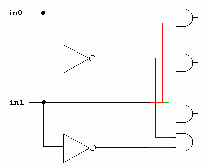
The red lines indicate the wires going to the AND gate at the top. The output of this AND gate will come on only when both inputs to the decoder are on. The green lines are for the second-highest AND gate, which will energize when the lower input is on, but the top input is off. The purple wires signify the AND gate which will activate when the top input is on but the bottom one is off, and finally, the blue lines lead to the AND gate for when both inputs are off. There are four possible combinations of input to this decoder, and each has a corresponding single output. A 3-to-8 decoder works the same way, except it would have eight AND gates at the right, three inputs, a NOT gate for each input, and more wiring.
Now that we know how to make a RAM cell, a tri-state buffer, and an address decoder, we have all the sub-circuits we need to make a complete, working RAM array. It's time to put it all together.
For this introduction, we'll illustrate a 4x2 SRAM array. RAM arrays are designated as bxw, where b is the number of bytes in the array, and w is the byte width, meaning how many bits are in each byte. Thus, our 4x2 RAM array has 4 bytes, and each byte contains two bits. (Most RAM arrays that you see in electronics parts catalogs will be somethingx8, because it's pretty typical to have 8 bits in a byte, but it's good to be different sometimes, and having only two bits to a byte makes things easier to draw, too.)
In an SRAM array, the RAM cells are arranged and wired up as follows:
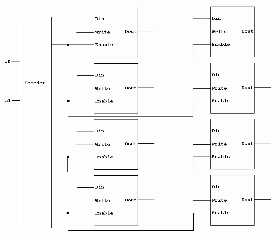
Typically, when diagrammed, a row of RAM cells represents one byte, and each column represents one bit in each byte. So in our 4x2 RAM array, we would have 4 rows (because we have 4 bytes total), and each row will have be two columns wide (because each has two bits):
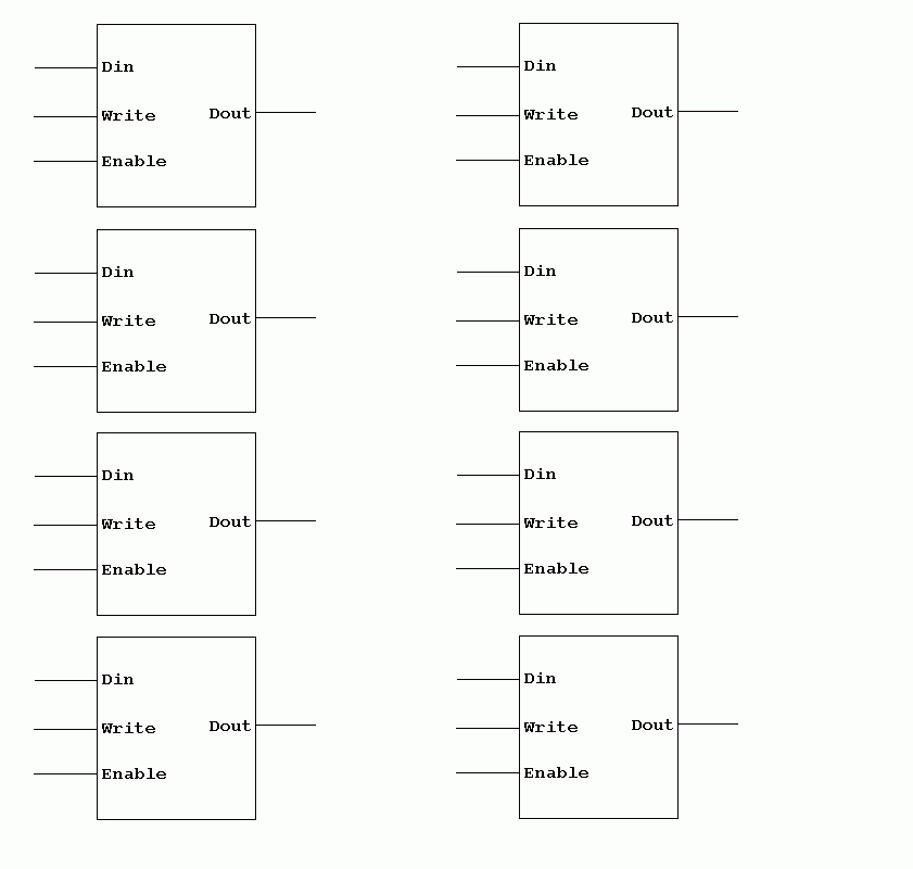
The Enable pins on the RAM cells lead from the outputs on the address decoder. Thus, each output on the address decoder goes to each RAM cell in one row of the RAM array (because you want to enable all of the bits in each byte when that byte is accessed).
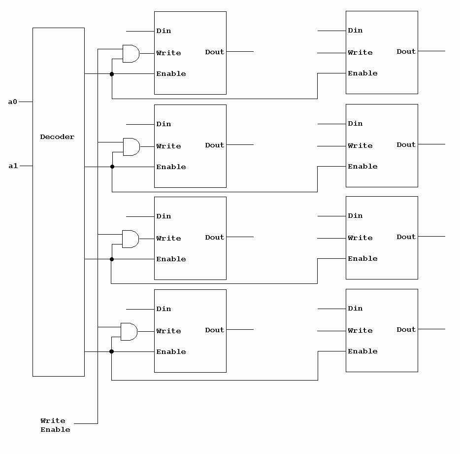
The outputs from the address decoder are also ANDed with the Write Enable signal to go to the cells' Write Enable pin. That way, when both a particular address AND the Write Enable signal are on, the data gets put into the cell. (Please note that at this point, I lost my patience with trying to draw all this, and so the picture below is only half-done; The output of the AND gate in each row should be going to the RAM cell on the right as well, but things got a bit too cluttered to provide any easy way for me to add this.)
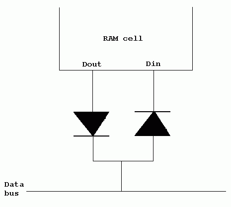
The only thing remaining is the data pins. They can simply be left as they are, to provide two separate data buses (one for data in, the other for data out), but microprocessors usually expect to use a bidirectional data bus. To achieve this, the data bus is connected to both the Data In pins and the Data Out pins of the RAM cells. This gives you a bidirectional data bus, but there needs to be a bit of additional circuitry added to this so that data only flows into the RAM array of out of it, but not both. And so we come to...
To ensure that data only flows in one direction at a time (either coming out of the RAM array or going into it), two diodes are used right next to each RAM cell, so that data only goes into it or out from it, but not both:
And there you have it. That's pretty much how RAM works. At least SRAM, anyway. And you don't really want to know how DRAM works, because DRAM sucks. Everybody should use SRAM and eliminate DRAM altogether.