Why?
Recently, I acquired an embedded board containing a
solid state
disk. The embedded board I've used allowed me to write files to the disk,
but I needed a tool that allowed me to completely format the solid state
disk. The only way I could achieve this was to build a board that allowed
me to mount the D.O.C 2000 on a normal PC.
Building your own
M-Systems had an ISA board, called the DIP Evaluation board (EVB), which
does exactly what I needed, but costs a few hundreds dollars.
As I was doing this for a hobby, I had no intention paying
this sum for a very simple board, so I decided to build one myself.
Since I had all sorts of old ISA cards I've decided to look for a card
which could be modified into a functional D.O.C 2000 programmer.
Warning!!!
The following section requires hardware understanding and good hands!
Do you understand?
If you have never done any soldering before, think twice before you do
this.
Are you still here?
Even if you have done soldering before, you will need here SMT soldering
skills!!!
Are you sure you want to keep reading?
If you blow up your computer and/or your board and/or your D.O.C
2000, you're on your own.
Still crazy enough to try this?
Although I've tried to keep this document error free as possible, the fact
is that this document was written, after I've finished building
my board, so I can't verify everything I've written here by building
another adapter, and I can't be 100% sure I haven't made any mistakes.
In no way I will take responsibility for any damage you might do by
following these instructions.
Use at your own risk!!!
Interfacing the D.O.C 2000
Before we present the board, let us start by understanding how the D.O.C
2000 works on a typical PC system:
From the system point of view, the D.O.C 2000 looks like a simple 8KByte
read/write memory.
When the PC boots, the PC BIOS looks in certain memory area for expansion
ROMs. These ROM are expected at predefined areas in the lower 1MB region,
Which can be accessed by all 8 bit ISA cards. These ROMs are identified by
a special signature found in the beginning of the ROM. Once this signature
is found, the PC BIOS calls this ROM to initialize it.
The DOC-2000 works by presenting itself as an 8KByte expansion ROM during
boot. Once the D.O.C-2000 ROM code is called, a BIOS expansion routine is
installed at the top of the memory, and a new BIOS-level hard disk is
added. In reality, this is not a hard disk, but a flash disk. The software
driver installed by the boot ROM code maps the BIOS hard disk read and
write operations into D.O.C 2000 operations. In order to access the flash
memory inside the D.O.C 2000, the ROM area can also be written, both to
select a page number (the D.O.C works using pages, like the old EMS
memory found in pre-AT PC's).
The pinout of the D.O.C 2000 can be seen in the following diagram:
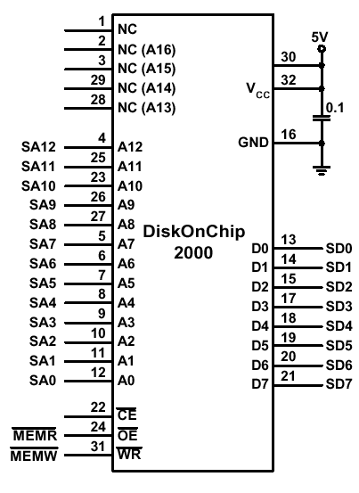
If we compare this with a typical 32KByte ROM, we will see the following
differences:
Picking up a card
What I really needed was a simple ISA card which already contained an
expansion ROM. I would then modify the card to provide a write signal
which the typical expansion ROM didn't require.
There are two common types of PC cards with expansion ROMs: Network cards
and SCSI cards. These cards usually supports booting the PC through SCSI
and Ethernet, and so they require a ROM to hold the device drivers
required.
I've looked through my arsenal of old PC card, and after looking at several
network cards, I ended up choosing Seagate's ancient 8-bit SCSI controller,
the ST-02. There are a few reasons why I've chosen this card:
- I had 2 of those.
- They were simple enough to modify.
What you would need
Here is a list of all the equipment you will need:
- An old Seagate ST-02 card.
- Two 32 pin DIP sockets, preferably of the round pin type.
- Some wire-wrapping wires and tools.
- Soldering tools.
Here is a picture of an original unmodified ST02 card (this is actually
the other card that I haven't modified, as I've taken these photos
after I've finished this work):

Work Instructions
Here are the step-by-step instructions for modifying your ST-02 card:
Remove the original EPROM
You can save the original EPROM if you would like to restore your ST-02
into working order someday.
Here is a picture of the ST-02 without the EPROM:
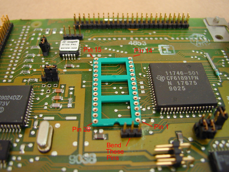 Notice the notch in the front of the EPROM socket. This notch marks pin 1
of the socket. If you hold the card with the notch pointing up, pin 1 is
the upper left corner, pin 14 is lower left, pin 15 is lower right, and
pin 28 is upper right.
Also notice the 3 pin header in front of the notch. You will have to bend
these slightly forward (or cut them out altogether) so that we can expand
the EPROM socket by 2 more pin rows without being obstructed by these pins.
Disable the I/O signals
The ST-02 use the ISA memory space for it's expansion ROM, but also use
some I/O addresses in the ISA I/O space for the SCSI and on-board floppy
controllers. Since we don't want the ST-02 floppy controller to interfere
with the PC's on-board floppy controller, we disable all I/O access to the
card.
In order to do this, we need to block two ISA signals: /IOR and /IOW.
Fortunately, there is a very simple way to do this, as can be seen in the
following picture:
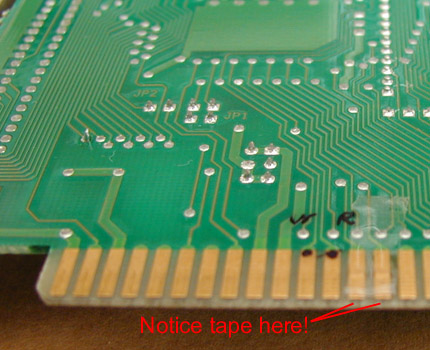
By placing transparent adhesive tape over the IOR and IOW pins on the ISA
connector (also known as B13 and B14 respectively),
we prevent the card from responding to any I/O read or write cycles,
effectively shutting down the on-board SCSI and floppy controllers,
as we wanted.
The IOR and IOW pins are identified by placing the board on the table with
the component side down, and counting the 13th and 14th pins from the left
side of the connector.
If you prefer, you can cut the traces coming out of the B13 and B14 pins
by a knife, instead of placing a tape over them. I prefer using tape
because the change is much more easily reversible.
Please notice that the pins marked by 'R' and 'W' are the /SMEMR and
/SMEMW lines, which are not masked. We will refer to these pins
later.
Solder wire-wrap wires
We would now solder 3 wires to control the three D.O.C 2000 pins: /CS, /OE
and /WR.
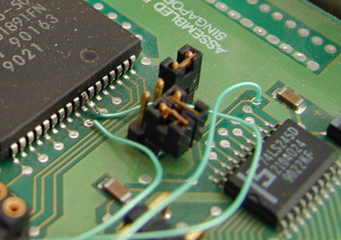
Solder 3 wires to the points above. The wires should be about 10cm long
each (that's about 4 inch for you americans!). We will trim the wires
later.
Preparing the conversion socket
Now we need to build the conversion socket that will help us adapt the 28
pin EPROM socket on the ST02 card to the 32 pin D.O.C 2000 socket.
Looking at the next pictures shows the similarities between these sockets:
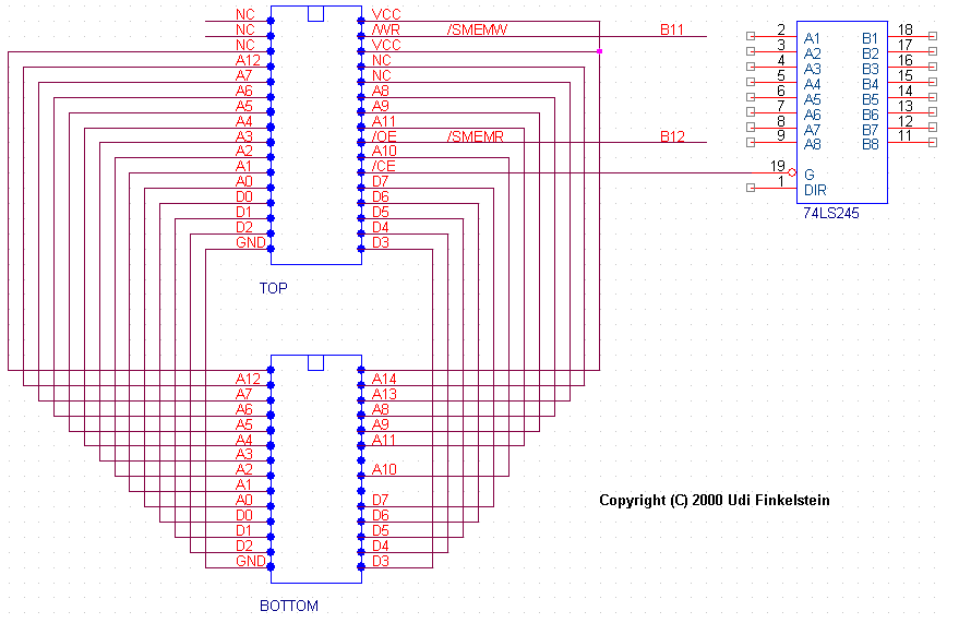
As we can see, If we align the two sockets on on top of each other, most
of the pins actually match:
- All the data pins, D0-D7.
- All the address pins, A0-A12.
- Ground.
Ofcourse, this is not a coincidence. A standard body called JEDEC, has set
standard pinout for memory components (EPROMs, SRAMs and Flash) in a way
that minimizes the amount of changes needed to be done on a PCB when
upgrading it from smaller memory chips to larger ones.
All the memory chips beginning with 2708 (1Kx8 EPROM) through the
27512 (64Kx8 EPROM) have shared common I/O pins as much as possible.
We will take advantage of this by building an adapter that converts the
32Kx8 EPROM socket on the ST02 to a D.O.C 2000 socket.
If we look at the diagram, we see that 95% of the signals are either
identical of driving Unused pins in the D.O.C. We only need to modify 4
pins:
- The D.O.C VCC pins.
- The D.O.C /WR pins.
- The D.O.C /OE pins.
- The D.O.C /CS pins.
In order to modify the pins, take one of the two 32 pin sockets we prepared
in advance.
Now we need to pull out some of the pins from the 32 pin socket. The pins
we really need to remove are those that are directly below the /CE and /OE
D.O.C 32 pin socket. If we hold the 32 pin socket and look at it from
above, with the notch being on top, we have pin 1 in the upper left corner,
pin 16 in the lower left corner, pin 17 in the lower right, and pin 32 in
the upper right.
Now, pull out the following pins: 1, 2, 22, 24, 31, 32.
using the round pin socket I had it was very easy to push out these pins.
Pins 1, 2, 32 were simply pulled out to make the socket fit on the
board.
Now we pass the wires we have prepared before in pins 22, 24, 31.
Please use the following picture to match the wires with the holes in the
socket.
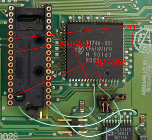
Please note that the picture above was taken later, and the marked pins
are obscured by the top socket, which we haven't gotten yet into!.
After the wires have been passed through the hole, push the socket firmly
into the board, on top of the EPROM socket.
Now take the second 32 pin socket, and do the following steps:
- connect a small wire wrap wire between pins 30 and 32.
- solder the wires coming through the first socket to the corresponding
pins in the second socket. Trim the pins as necessary to make it fit.
- push the second socket on top of the first socket.
We now have a functional D.O.C 2000 adapter!
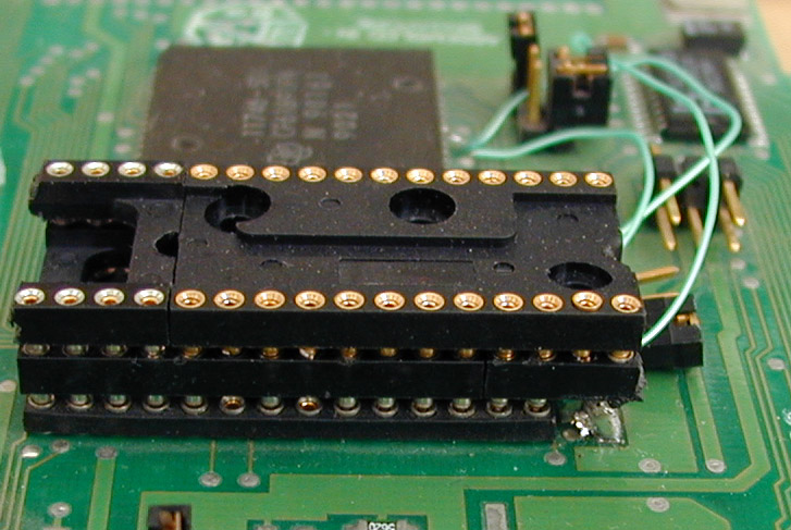
Please take a look at the following pictures. Your adapter should look
similar, but not the same:
- I've connected the VCC pin (32) directly to the capacitor below it
instead of using pin 30 (don't do this, was this wasn't very smart).
- I didn't have two 32 pin sockets, so I made one from scrapes of shorter
sockets.
Here is a look from the side:
And another one from the opposite side:
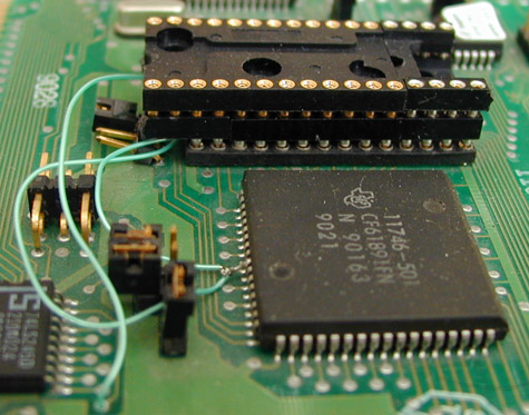
Testing the board
Download the
DiskOnChip software Utilities from the M-Systems web site,
as well as the
DiskOnChip software Utilities User's Manual. Please follow the
instructions there, since the card should behave the same.
Using this board with the DiskOnChip Millenium
The DOC Millenium has an identical electrical interface as the D.O.C 2000,
so it should work with this board as well. However, I haven't tried it.
As usual, try this at your own risk.
Disclaimer
If you have gone this far, I assume that you know what you're doing.
See the warning in the beginning of thus document.
This is also the point I got tired writing...
This page has been accessed
 times since Jul 28, 2000.
Copyright © 2000 Udi Finkelstein
, All Rights Reserved.
"Last updated:
 times since Jul 28, 2000.


 Notice the notch in the front of the EPROM socket. This notch marks pin 1
of the socket. If you hold the card with the notch pointing up, pin 1 is
the upper left corner, pin 14 is lower left, pin 15 is lower right, and
pin 28 is upper right.


 times since Jul 28, 2000.