A DAC of the Klones!
Introduction
Mr. Kusunoki developed the Non-oversampling, Digital-filter-less DAC Concept, which has been adopted by 47 Laboratory for the Progression and Shigaraki DAC. A couple of DIY projects along the same lines also exist, notably A. Galavotti's Zero and Minimo as wel as the well documented TNT-audio Convertus.
The basic 16 bit / 44.1kHz encoding of the CD is left unaltered during the entire digital to analog conversion. No oversampling or filtering is used. The digital word is converted to its equivalent voltage on a sample by sample basis. While this seems like a purist approach, the output signal is far from pure: what should be smooth waveforms look like a series of jagged steps. The reason the DAC works at all is because our ears - and our equipment downstream to some extent - provide the filtering: the jagged steps produce noise at frequencies well above what we can hear, or what most speakers can reproduce.
The philosophy, which you will either accept or not as you want, is that given that the CD sampling rate requires a filter which cuts nothing at 20 kHz but everything at 22 kHz, and given an electronic implementation of such a steep filter in either in the analog or digital entails serious side effects, the best option is to leave the filtering to the acoustic transducers: loudspeakers and the ear.
It should be said that some loudspeakers, and some ears, do this filtering better than others. The stepped waveform may cause audible distortion in some electronics. This DAC is not for everyone.
Circuit Overview
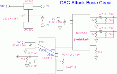
At 20 total parts, it is clear than anything not indespensible was dropped. 2 chips, 2 voltage regulators, 7 resistors, 9 capacitors. The SPDIF output from the transport is de-multiplexed by the crystal CS8412 receiver, which reclocks the data and outputs the digital signal to the 16 bit Philips TDA1643 DAC. The DAC outputs an analog current proportional to the digitally encoded input signal, and the current is drawn through the output resistors, one for each channel, to produce the output voltage.Download the datasheet for the Crystal CS8412 receiver ( cs8411.pdf ) and Philips TDA1543 DAC ( tda1543_cnv_2.pdf ).
The TDA1543 is run at 9 V instead of the normal 5 V. This is done to give the chip enough headroom to output a standard 2 Vrms output signal. The result will be a dangerously warm chip unless heatsinking is used.
The CS8412 needs to be set to MODE 2 (I2S output) so set M3-M0 as follows: M3(pin17) = GND, M2(pin18) = GND , M1(pin24) = 5 V , M0(pin23) = GND. Pin 13 should also be grounded.
Design and Layout
The 47 Laboratory DACs are built on a 30 mm x 35 mm circuit board, almost certainly using SMT (surface mount technology) chips and possibly SMT resitors as well. Standard DIP / DIL packaging for the chips is available, and although a larger layout will be unavoidable, the bigger components are much easier for the typical DIYer to deal with.
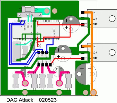
This suggested layout uses standard size components and DIP chips. It is a single layer, single sided board. You are looking at it from the top, solder side down, in X-ray view. DAC and Vregs are on the bottom, solder side, everything else is on top. Board secured by the Vregs, which presses the DAC against the case for heatsinking. (n.b. use thermal grease.)
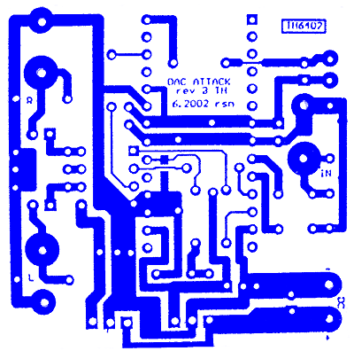
Scott Nixon has designed a neat layout. Here is the solder side DIP/through hole version 3. Its not available anymore, but he's still selling related products.


|

