The Twilight Amplifier
A MOSFET mu-follower for headphone listening.
Introduction
This circuit comes from the original article on the mu-follower by Alan Kimmel:
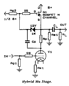
It's a triode voltage amplifier with a MOSFET constant current source (CCS) as the plate load. The MOSFET also provides a low impedance, relatively high current output for driving the headphones.
The Amplifier Circuit
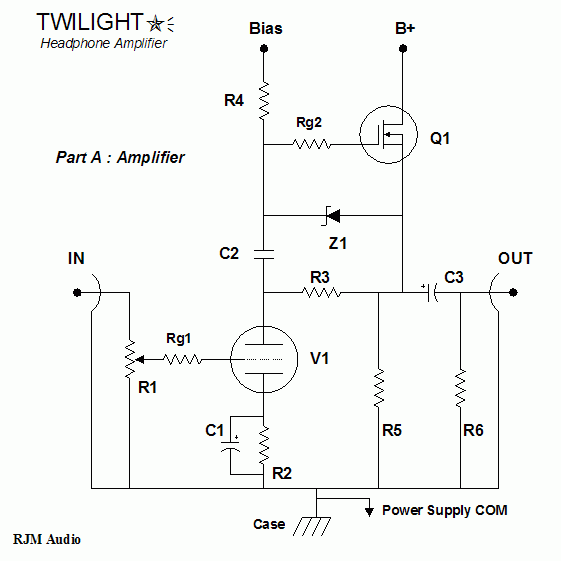
The output stage is made up of the MOSFET, Q1, configured as a source follower with R5 as the source resistor. The headphone load is connected through the coupling capacitor C3. This part is essentially a Szekeres headphone buffer. The gate of the MOSFET is driven by the plate of the triode, V1, through the coupling capacitor, C2. The triode is a simple voltage amplifier. The plate resistor R3 is tied to the MOSFET source in a constant current configuration, rather than to the B+ directly, and this innovation is what makes it a mu-stage circuit. The triode borrows some of the MOSFET's strength to increase the effective plate resistance, lowering distortion. The tradeoff is the MOSFET source has to sit at the plate voltage, more or less, so the source resistance R5 dissipates a lot more power that it would otherwise. This is not an efficient circuit.
| Component | Value | Description |
|---|---|---|
| B+ | 70 V | Power supply voltage. |
| Bias | 60 V | Bias supply voltage |
| R1 | 10k / log | Volume attenuator. |
| Rg1 | 1k | Optional grid resistor. |
| R2 | 2k | Cathode resistor. |
| Rg2 | 1k | Gate resistor for the MOSFET, usually needed. |
| R3 | 4.7k | Plate resistor for V1. |
| R4 | 470k | Ties the MOSFET gate to the bias voltage. No current flows so the value can be very high. |
| R5 | 1.5k 5W | Source resistor for Q1. Smaller values give higher circuit current, more output power, and dissipate more heat. |
| R6 | 47k | Ties the output to ground, exact value not critical. |
| C1 | 47µF 16V | Cathode bypass capacitor. |
| C2 | 0.47µF 200V | Coupling capacitor. |
| C3 | 100µF 100V | Output coupling capacitor. Bass cutoff depends on time constant C3 x HeadphoneZ. |
| V1 | 1/2 6CG7 or 6SN7 | |
| Q1 | 2SK213 | p-channel, enhancement mode power MOSFET. A low distortion MOSFET designed to be used in audio rather than switching applications. IRF510 may be substituted. |
| Z1 | 12 V Zener | Protection diodes are built in to the 2SK213, but for the IRF510 this zener will limit the gate voltage from getting more than 12 V above or 1 V below the source voltage. An unprotected MOSFET will generally fail if the gate-source voltage exceeds 20 V in either direction, a situation that might occur on power-off. |
The gain of the circuit is defined by the mu of the vacuum tube. This will be about 20 for the 6SN7-6CG7 family. The output impedance will depend mostly on the transconductance of the MOSFET, its about 10 ohms with the 2SK213. The output power depends on the value of R5, the power supply voltage, and the headphone impedance. It's about 40 mW (<1% distortion) into 300 ohms, only 10 mW is available into 32 ohm loads however. The heat dissipated depends on the value of R5 and the power supply voltage. Its about 5 Watts, not including the tube filament.
Power Supply
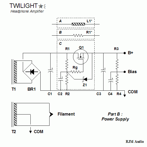
As shown by options A, B and C in the power supply diagram below, a low-ripple B+ voltage can be achieved by conventional RC filtering, an inductor, or a MOSFET line smoother.
| Component | Value | Description |
|---|---|---|
| R1 | 47k | |
| R2 | 220k | With R1 forms a voltage divider to bias the MOSFET, dropping the output voltage by R1/(R1+R2). |
| R3 | 47k | |
| R4 | 220k | With R3 forms a voltage divider to bias the gate of MOSFET of the mu-follower. |
| Rg | 1k | Gate resistor for the MOSFET, usually needed. |
| C1 | 100µF 100V | Input capacitance should be kept low. |
| C2 | 100µF 100V | Bypasses R2. A large value has the side benefit of a long turn on time, effectively a soft start circuit for the B+. The time constant is approximately R1xC2, about 5 seconds in the present case. |
| C3 | 100µF 100V | Increase as needed to reduce output ripple. I had no problem with using the values shown. |
| C4 | 100µF 100V | Bypasses R4. A large value has the side benefit of a long turn on time, effectively a soft start circuit for the B+. The time constant is approximately R1xC2, about 5 seconds in the present case. |
| T1 | 60 VAC secondary / 0.25 A | |
| T2 | 6 V ct / 5 VA or 6.3 V ct / 3 VA filament transformer | The 6CG7 heater draws 600 mA, so over-sizing a6 V transformer should increase the voltage 5% or so to get the just the right amount for the heater. If 6.3 V is used and the voltage ends up too high, connect a pair of small value resistors (0.22 ohms for example) in series with the heater. |
| BR1 | Rectifier diodes | Anything rated to 400V 1A or better. |
| Z1 | 12 V Zener | For the IRF 510 or IRF610 attach Z1 between gate and source to protect the inputs during shut down. Not required with the 2SK213. |
| Q1 | 2SK213 (IRF510 or IRF610 can be substituted). | |
| L1* | 10 H | A choke filter. |
| R1* | 470R 2W | A simple CRC filter will probably work, but the values of C1 and C3 will have to be significantly larger. |
There is obviously a lot of flexibility in the design of the power supply. It can be true dual mono, or some of all of the components can be shared between channels. If the power supply is dual mono the filter capacitance values can be halved.
With AC filament heating a transformer with a center tap or two 3.3 V secondaries should be used for hum cancelling. DC heating can also be used.
Construction Notes
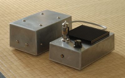
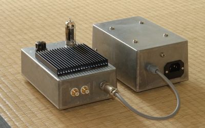
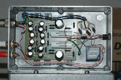
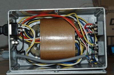
I designed a circuit board to accomodate most of the parts. The triode and the grid and cathode resistors are off-board and wired point-to-point. The Eagle .brd and .sch files can be downloaded here. They are my working files, so the values shown do not exactly match the published schematic. Note that the IRF510 and 2SK213 are not pin-compatible, and that this board is drawn for the 2SK213.
The photos show the ALPS volume potentiometer which was replaced later with a stepped attenuator. The cathode bypass capacitors were not installed at the time the photo was taken, but added later.The transformer was custom made for me by Pheonix Corporation in Japan. It is R-core type, 80 VA, with 2x60VAC-0.4A and 6.3VAC-1A C.T., and comes with an electrostatic screen. The transformer and diodes were configured as an a outboard power supply, while the filter capacitors and line smoother were with the rest of the amplifier circuit in the main case. The power supply umbilical was made from seven conductor unshielded cable, with a small 7 pin bayonet connector on the amplifier side. Electrolytic capacitors are Black Gate Std. Coupling caps are Multicap PPFXS. Resistors are mostly Holco, with Riken Ohm and Caddock for the cathode and source resistors, respectively. Cast aluminum cases are made by Hammond Mfg.
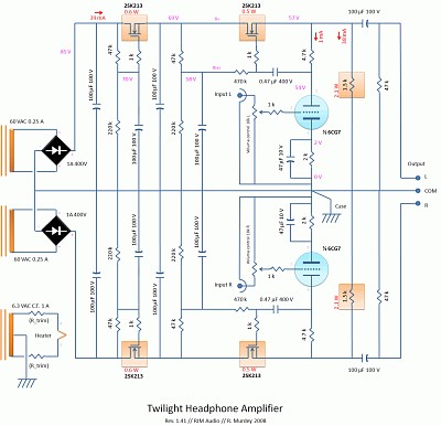
Here is the complete circuit diagram, configured more or less as I built it:
The amplifier inverts signal polarity. There is no audible hum or noise, even with AC filaments. 60 Hz and 120 Hz hum and ripple are below -80 dB (100 µV). THD is 0.1% for 5 mW and 0.01% for 0.5 mW, with the second harmonic dominating. This is not an easy project, some parts are hard to source and the construction can be a bit of a pain, but in my opinion it is well worth the effort.
rjm003.geo at yahoo.com

|
