

A diode is a "one way valve" for electricity. It is a semiconductor composed of silicon or geranium, containing a PN junction. The end of the diode that is an arrow is called the anode (P-type crystal), and the line end is called the cathode (N-type crystal).
A semiconductor is a material that conducts electricity to some extent. It is not a very good conductor, and not a good insulator, but somewhere in between. A conductor lets electricity pass through easily, while an insulator does not allow electricity to flow well. In order for a material to conduct its valence electrons must be in the conduction band. In conductors it takes no energy to move the valence electrons into the conduction band, because they overlap, and they are ready to conduct electricity anytime. In insulators there is a gap between the valence band and conduction band. This gap is termed the forbidden gap, and it takes a certain amount of energy to move the valence electrons across it to enter the conduction band. The larger the forbidden gap, the more energy it will take to move the valence electrons into the conduction band. It takes a large amount of energy to cause insulators to conduct, but doing so can destroy the material. In semiconductors a small forbidden gap exists. It does not take such a large amount of energy for them to begin conduction.

In a semiconductor, the silicon or geranium is doped, which is the process of adding impurities, to form N-type and P-type crystals. These impurities have a different number of valence electrons than geranium or silicon, which have four. Trivalents, which have 3 valence electrons, are added to the geranium during crystallization to create a P-type crystal. If you were to look at the structure of the covalent bonding in the crystal, you would see many bonds between the silicon, or geranium, where all four valence electrons are paired up with an adjacent molecule. But where there are trivalents, only 3 molecules are paired up with it, leaving a hole, which is a positive site, the majority carrier for the P-type crystal. These dopants that create holes are called acceptor impurities, because the holes accept electrons. The same process is used for the N-type crystal, but pentavalents are used, which have 5 valence electrons. So when the silicon or geranium crystallizes, four molecules bond covalently with the pentavents, and the fifth valence electron does not bond with anything and creates a negative site, the majority carrier for the N-type crystal. These types of dopants that add electrons are called donor impurities, because they lend electrons.

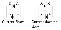
If the positive terminal of a battery is connected to the anode, and the cathode is connected to the negative terminal, the diode is forward biased, and the current can flow through it. If the diode is reversed, and the cathode is connected to the positive terminal, and the anode is connected to the negative terminal, the diode is reverse biased, and very little current flows. Note that when the diode is forward biased, it is pointing + to -. For this reason it is easier to think in terms of conventional flow (+ to -), rather than electron flow (- to +).
The reason electricity only flows well in one direction is because a negative current moving in an P-type crystal is attracted to the positive holes, and pairs up with them. And a positive current is attracted to the electrons, and pairs up with them. This decreases the amount of current carriers in the crystal, and increases a region across the junction called the depletion area (also called the space charge region and transition area). This is a region where current carriers are void due to the electron hole pairs. This region occurs naturally due to electrons from the N-type crystal crossing the junction to form electron hole pairs with the holes in the P-type crystal, and from holes moving across the junction to form electron hole pairs with the electrons in the N-type crystal. A voltage forms across the diode called the potential hill, or barrier, caused by the electrons and holes crossing over the junction. The N-type crystal becomes positive from electrons leaving and holes entering, and the P-type crystal becomes negative from holes leaving and electrons entering. If the diode is in reverse bias, this potential hill will be in the same polarity to the voltage across it, and block the flow of electricity. But a very small current does flow through the diode in reverse bias due to minority carriers. The minority carriers in the N-type crystal are holes, and in the P-type crystals, electrons. In N-type crystals, the holes are formed from holes in electron hole pairs, and in P-type, freed electrons from electron hole pairs. But the reverse bias current across the diode is very small. When the diode is forward biased the negative current flows through the N-type crystal, and the electrons are not attracted to one another, so the current flows right through. The same goes for the positive current moving through the P-type crystal. This decreases the depletion area, and potential hill allowing the flow of electricity.
A zener diode works the same way as an ordinary diode, except that it will also conduct in reverse bias when a certain voltage is reached. The voltage at which the reverse bias breakdown occurs is called the zener voltage. Zener diodes are commonly used in power supplies to regulate the output voltage. If the voltage becomes too high, the zener diode will begin to conduct, and decrease the voltage, then cease conduction when the voltage drops low enough.

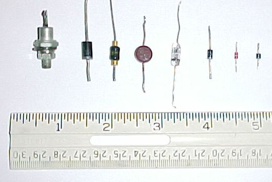
A picture of some diodes is shown above. The cathode of many of the diodes is marked
with a band, while others have a schematic of the diode showing which end is the
cathode, and which end is the anode. Larger diodes, such as the one on the far left,
contain heat sinks, which doubles as the anode/cathode of the diode.
Another way you might look at a diode is a waterfall. The top of the waterfall is the higher energy N material, and the bottom is the lower energy P material. The water can only flow from the N to P junction, not the other way around. Unless the voltage is high enough, the water will be high enough to cross the other way. In a zener diode this can be done without destroying the diode, but a in a regular diode the junction may be destroyed.