HOME PREVIOUS NEXT

Creating top-down design

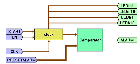
A simple alarm clock design is used to demonstrate top-down design using the VHDLMG. Select the top item in the design hierarchy explorer, add a new module named "alarmclock". Follow the block diagram below to build the top level alarm clock design. The clock module is now a black box that counts the time. It has 4-digit outputs (2 for minute and 2 for hour) in both 7-segment display format and BCD format. The "EN" signal triggers the clock to count every minute. A library module, comparator, is used in this example. Insert it from Arithmetic category in the module library. The module compares BCD outputs from clock with the input alarm preset value, PRESETALARM. If they are equal, ALARM signal becomes high.

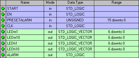
Fill in the interface port list of the alarmclock module and organize the sequence as in the list below.

Set the parameters of the Comparator as in figure below:

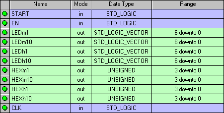
Set the interface ports of the clock module as below:

Analyze the alarmclock module and then open its VHDL file. Add the following code to the file.

architecture alarmclock_arch of alarmclock is

    signal HEXm1,HEXm10,HEXh1,HEXh10 : UNSIGNED(3 downto 0);
    signal BCDhhmm : UNSIGNED(15 downto 0);

    ....
    ....

begin

    U_clock: clock
        port map (START, EN, LEDm1, LEDm10, LEDh1, LEDh10, HEXm1, HEXm10, HEXh1, HEXh10, CLK);

    BCDhhmm <= HEXh10 & HEXh1 & HEXm10 & HEXm1;

    U_Comparator: Comparator
        port map (A=>BCDhhmm, B=>PRESETALARM, EQUAL=>ALARM);

end alarmclock_arch;

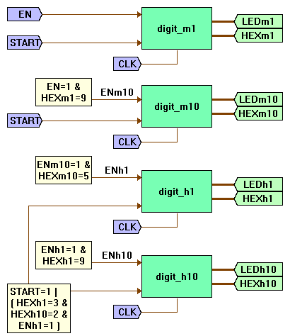
Now, move down to the clock module. Create block diagram as shown below. The library modules digit_m1, digit_m10, digit_h1, and digit_h10 are taken from the digit module stored in module library previously. After inserting the modules, rename them by selecting the module, then hit space bar and key in a new name accordingly. Renaming can be done either in design hierarchy explorer or block diagram editor. The light-yellow blocks are custom blocks for illustration purpose.

Set the EndValue parameter at the digit modules as follow:
Module EndValue
digit_h10 2
digit_h1 9
digit_m10 5
digit_m1 9

Open the VHDL file of clock module and add the following code to the file.

architecture clock_arch of clock is

    signal ENm10,ENh1,ENh10: STD_LOGIC;
    signal HEXm1i, HEXm10i, HEXh1i, HEXh10i: UNSIGNED(3 downto 0);
    signal STARTh :STD_LOGIC;

    ....
    ....

begin

    U_digit_m1: digit_m1
        port map (START, EN, HEXm1i, LEDm1, CLK);
    HEXm1 <= HEXm1i;

    ENm10 <= '1' when EN='1' and HEXm1i=9
        else '0';
    U_digit_m10: digit_m10
        port map (START, ENm10, HEXm10i, LEDm10, CLK);
    HEXm10 <= HEXm10i;

    STARTh <= '1' when START='1' or (HEXh1i=3 and HEXh10i=2 and ENh1='1') else '0';

    ENh1 <= '1' when ENm10='1' and HEXm10i=5
        else '0';
    U_digit_h1: digit_h1
        port map (STARTh, ENh1, HEXh1i, LEDh1, CLK);
    HEXh1 <= HEXh1i;

    ENh10 <= '1' when ENH1='1' and HEXh1i=9
        else '0';
    U_digit_h10: digit_h10
        port map (STARTh, ENh10, HEXh10i, LEDh10, CLK);
    HEXh10 <= HEXh10i;

end clock_arch;

Then, close the file and analyze the alarmclock module. If no error is encountered, you have done the top-down design successfully. Generate synthesizable VHDL file for the alarmclock module, and run the synthesis, implementation, and simulation processes to verify the design.


HOME PREVIOUS NEXT
1