The Szekeres VE
A direct-coupled, single-stage, single-ended MOSFET follower for headphone listening.
VE: Virtual Engine
This project is another followup to Greg Szekeres' MOSFET Buffer at Headwize. The original was a simple unity gain follower using one MOSFET per channel. Conceptually simple, but in practice a couple of unwanted but necessary complications arose: coupling capacitors were needed on both the input and output, and a regulated power supply was required due to the inherently poor power supply rejection. Greg had already forseen the solution, however. At one point in the article he writes:
One thing I didn't try was to use two circuits per side, so one could use direct coupling on the output side by feeding the signal to one side, and using the other side to provide a positive but equal resting voltage creating an effective zero-DC operating point.
He went on to say that he didn't bother because he wanted to keep things simple. In light of the final circuit he ended up with, though, I didn't see it that way. First, since a standard headphone jack has a shared common only one extra circuit is needed, not two. Second, driving the headphone common with a dedicated MOSFET stage cancels most of the power supply noise at the same time as it enables a DC-coupled output. If, in addition, a split power supply is used the MOSFET gates can now be left at the potential of the signal common. No input coupling capacitor is needed, and no biasing circuitry, either. The output noise is sufficiently reduced over the original design that a regulated power supply is no longer needed. All this radically simplifies the execution, more than enough, I think, to justify that extra MOSFET circuit.
As with the original, this is a buffer stage, not a complete amplifier. There is no volume control and no voltage gain. Thus it should be driven directly by a preamplifier line output, the headphone output from a computer or portable audio player, or similar source equipped with volume control.
The Circuit
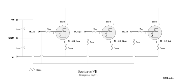
As shown in the schematic below three MOSFET follower units are used. One for the right channel, one for the left, and the extra one for the virtual output common. All three outputs measure about -1 V, hence the output offset voltage across the headphone load is zero. Power supply ripple and noise also cancels out across the headphone output, to the extent that it is equally present on each channel. In practice there is a small imbalance due to manufacturing differences in each MOSFET that can be minimised by carefully matching of the gate-source voltages.
The best MOSFET to use is probably the Renesas (Hitachi) 2SK213 (also 2SK214, 2SK215, or 2SK216) (datasheet). It is designed for audio amplification at relatively low current, has a low input capacitance of only 90 pF, and has gate protection diodes built into the package. The IRF510 (datasheet) is the more widely available substitute, though please note it is not pin compatible with the 2SK213. The circuit layout must be changed slightly, and the addition of gate protection diodes is recommended.
Examining the rest of the components:
The input resistors, R_input, define the practical input impedance of the circuit. 22 kohms (10 kohm - 100 kohm) is a typical value for the right and left channel. No resistor is used at the input of the virtual channel since the signal ground connects directly to the circuit common.
The gate resistors, R_gate, limit the high frequency bandwidth, preventing oscillation. A suggested value is 470 ohms (100 ohm - 1 kohm). The higher the gate capacitance, the lower the gate resistance. So, 100 ohms is perhaps a better choice when using the IRF510.
The source resistors, R_source, together with the power supply voltages set the operating current and power draw. The lower the resistance, the hotter everything will get unless the power supply voltage is lowered, too. R_source should be similar in value to the impedance of the headphone load. 100 ohms is a good general-purpose value. Source resistors should be matched to within 1%.
Next, the power supply voltages should be determined. ±9 V is a good general-purpose target. This, with R_source = 100 ohm, will result in 75 mA per channel and a total power draw of 4 W for the complete three-channel circuit. The output power is at least 50 mW into all headphones between 30 ohms and 300 ohms. Although 4 W doesn't sound like a lot, a fairly chunky heatsink will be needed to keep eveything cool. In addition the source resistances should be rated to at least 1 W, though the other resistors can be 1/4 W types.
The capacitors, assuming an unfiltered, unregulated power supply, should be at least 2200 µF. With a regulated power supply much smaller values can be used.
This worksheet (Excel file, zip compression) shows how the output power and depends on the source resistance, power supply voltages and headphone impedance. It also calculates the amount of heat that must be dissipated by the heatsinks and chassis.
Power Supply
A split supply is needed, with both positive and negative rails. As the virtual channel cancels the power supply noise at the output, the power supply ripple can much higher than for the normal Szekeres circuit. It is quite possible to use an unregulated supply with no additional filter capacitors ... i.e., just a transformer and diodes. Recommended transformer: Amveco 62080, 2x7 VAC, 50 VA.
Layout
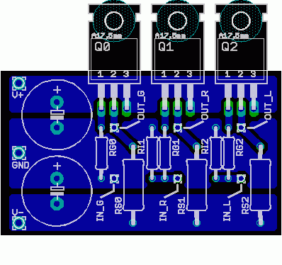
The circuit is very compact. An example layout is shown below. The large source resistors could be mounted on the bottom of the board so they touch the heatsink for better cooling. The MOSFETs are fixed to the heatsink through an insulating pad.

It is very important that the MOSFET substrates are isolated from the physical case and from each other, and also that the headphone common signal, which is at -1 V, is isolated form the case. In many headphone sockets the ground ring is electrically connected to the chassis mount, if this is the case a plastic spacer or some such must be used between the socket and case.
Construction Notes
The final version was built from the following components: Renesas 2SK213 MOSFETs current matched to 1%, R_in = 20 kohms (Holco 1/2W), R_gate = 470 ohms (Holco 1/2W), R_source = 390 ohms (Caddock MP-930 in TO-220 package). C_filter = 1000 µF (Nippon Chemicon KMG). Power supply was the same external toroidal transformer and diodes I use with my Gainclone, 2x12 VAC, 160VA, Electrostatic screen and magnetic shield.

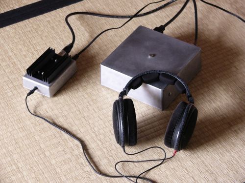
Also: Photos of the internal layout and underside of the board.
The operating point I used is optimised for my 300 ohm headphones. For a nominal power supply voltage of ±15 V, the output power is 60 mW + 60 mW into 300 ohms, and the total heat is 3 W. The measured DC offset was less than 5 mV. The output hum+noise was below measurement threshold of 0.6 mV, and inaudible.
I emphasise again that the configuration I used is optimised for 300 ohm loads and the power supply that was available to me. Normally you should use the following recommended configuration instead: ±9 V, R_source = 100 ohms, C = 2200 µF.
Lastly, a word about matching MOSFETs. The procedures described here [PassDIY] are probably the simplest. Set the resistance to draw the same current as your circuit. The three MOSFETs to be used should measure no more than 50 mV apart. For 2SK213 parts from the same manufacturing batch, measuring and selecting from a group of only four or five parts should yield at least three with this level of tolerence. Use the middlemost value for the common channel.
rjm003.geo at yahoo.com

|
