|
|

Convert Analog into Digital Challenge
Surfing on the net,
visiting websites connected to electronics, I also visited TI. I noticed the
banner “Convert Analog to Cash – TI $60,000 Analog Design Challenge “ .
It sounded interesting to me, so I decided to find out more...and here is my
journey...
This competition
was organized by TI together with other sponsors. The money fond
for rewards was $60.000. First price was $5.000. Many of the
rewards were components, software, books, developing tools.
The article is a description of my project, sent to TI, for the
competition. I also provided two files bellow, the sch and pcb
files. You can download them at the bottom of this page.
PWM
generator
This
construction can be used for generating signal with
constant frequency but with variable signal-pause ratio. This
signal have average voltage proportional with duty cycle. So, we
can say that this construction is digital to analog converter.
Variable ratio between signal and pause is 1:100 with resolution
1%. The frequency is quite stable which depends on accuracy of
the crystal in the clock oscillator. Frequency of CLOCK is not
critical. I recommend clock frequency 2,5 MHz. After passing
through two counters, clock frequency will be divided by 100,
and the output PWM signal will have the frequency of 25kHz. This
frequency is above audio range and is appropriate for DC motor
controlling purposes. Desired signal-pause ratio can be set by
two BCD digital switches. The number we set on the digital
switches represents
duration of signal (logic “1”). Practically, if we want to
produce signal with 36% of logic “1” and 64% of logical
“0” we must set the switches on number 36. The switches must
be BCD switches. It is important not to make mistakes and take
hexadecimal switches with sixteen positions.
Besides
power supply (5V), there is input for CLOCK and the outputs for
the signals we make (Q) and `Q
(same signal but inverted).
Signal
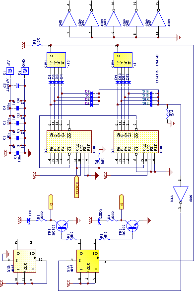
CLOCK is connected to the inputs of
counters U2 and U3. The carry out pin of U3 is connect to
the carry in pin of U2. These counters count up to 100. Those
outputs are connected on pin 3 of U4 through the diodes D5-D8
and D13-D16. Common pins of switches, witch are usually assigned
with “C” or “COM”,
are connected through R5 to the +5V. In the moment of
switching on, the logic levels on all outputs are zero. This
level sets U1A on pin 7. The state on output Q changes from 0 to
1. This state remains till the counting number becomes the same
with set up number. In that moment, the level on pin C on BCD
switches fall on logic 0 and U1A will be reset on pin 4. This
transition represents the beginning of pause in output signal.
When counters count up to 100, U1A will be set on pin 7.
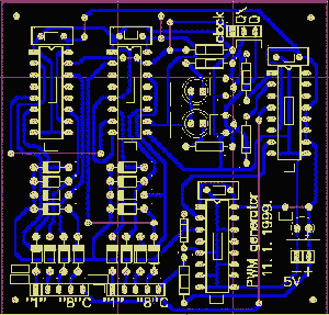
The
circuit board is single layer with jumpers.
Download:
(pcb & sch)
written by:
el. eng. Velja Cvetković,
Capture
of SCH:

Capture
of PCB:

|
©  |
|
|